- 您现在的位置:买卖IC网 > Sheet目录329 > IDT70V525ML55BZI (IDT, Integrated Device Technology Inc)IC SRAM 128KBIT 55NS 144FBGA
IDT70X525XML
Low Power 4K x 8 TriPort Static RAM
AC Electrical Characteristics Over the
Operating Temperature and Supply Voltage
70X525X
Ind'l Only
Preliminary
Industrial Temperature Range
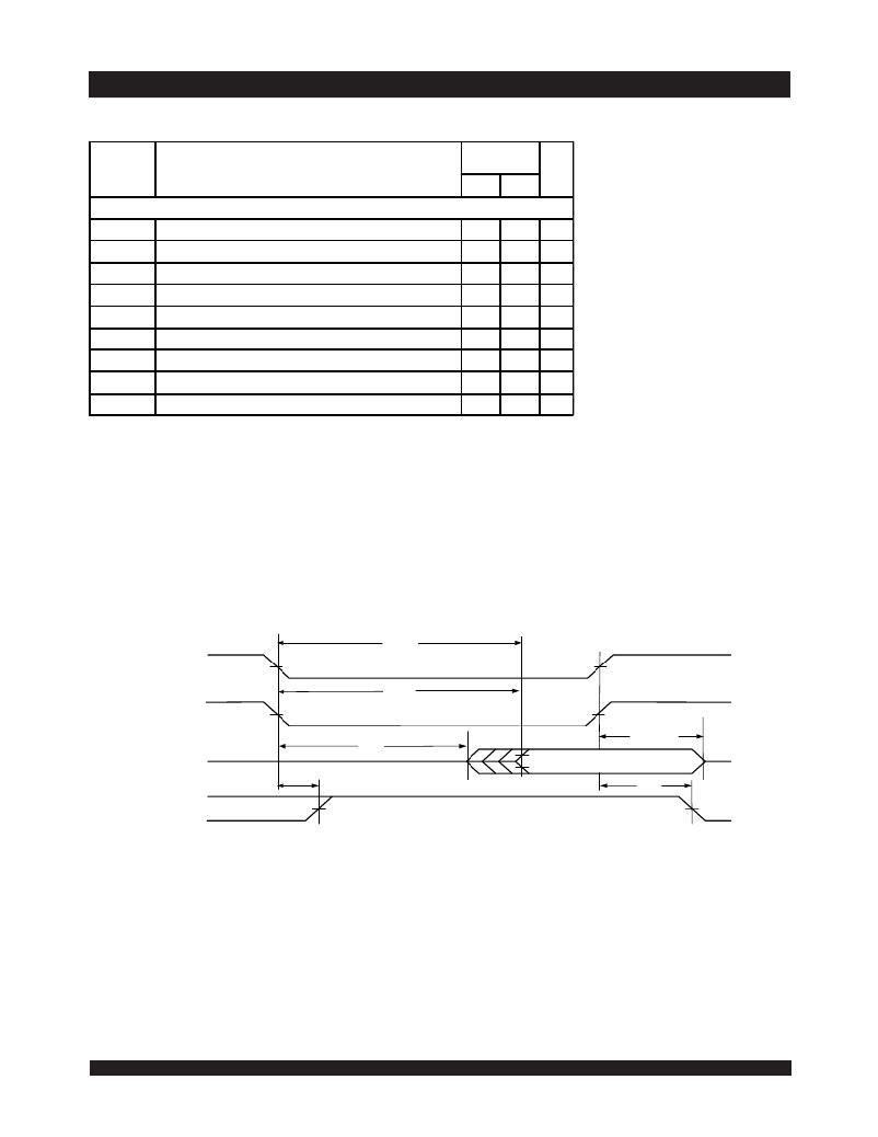
Symbol
Parameter
Min.
Max.
Unit
READ CYCLE
t RC
t AA
t ACE
t AOE
t OH
Read Cycle Time
Address Access Time
Chip Enable Access Time
Output Enable Access Time
Output Hold from Address Change
55
____
____
____
5
____
55
55
30
____
ns
ns
ns
ns
ns
t LZ
Output Low-Z Time
(1,2)
5
____
ns
t HZ
Output High-Z Time
(1,2)
____
25
ns
t PU
Chip Enable to Power Up Time
(2)
0
____
ns
t PD
Chip Disable to Power Down Time
(2)
____
55
ns
NOTES:
5681 tb10
1. Transition is measured 0mV from Low or High-impedance voltage with the Output Test Load (Figure 2).
2. This parameter is guaranteed by device characterization but is not production tested.
Timing Waveform of Read Cycle No. 2, Any Port (1, 2)
t ACE
CE x or BE x (3)
OE
t AOE
DATA OUT
t PU
t LZ
(4)
VALID DATA
t HZ
t PD
(5)
I CC
CURRENT
I SB
50%
50%
,
5681 drw 08
NOTES:
1. R/ W = V IH for Read Cycles.
2. Addresses valid prior to or coincident with CE (or BE x) transition LOW.
3. CE for Port 2 or Port 3, BE x for Port 1.
4. Timing depends on which signal is asserted last, CE (or BE x) or OE .
5. Timing depends on which signal is deasserted first, CE (or BE x) or OE .
8
6.42
发布紧急采购,3分钟左右您将得到回复。
相关PDF资料
IDT70V5388S166BGI
IC SRAM 1.125MBIT 166MHZ 272BGA
IDT70V631S10PRFG
IC SRAM 4MBIT 10NS 128TQFP
IDT70V639S12PRFI
IC SRAM 2.25MBIT 12NS 128TQFP
IDT70V659S12DRI
IC SRAM 4MBIT 12NS 208QFP
IDT70V7319S166BCI
IC SRAM 4MBIT 166MHZ 256BGA
IDT70V7339S166BCI
IC SRAM 9MBIT 166MHZ 256BGA
IDT70V7519S166DRI
IC SRAM 9MBIT 166MHZ 208QFP
IDT70V7599S133DRI
IC SRAM 4MBIT 133MHZ 208QFP
相关代理商/技术参数
IDT70V525ML55BZI8
功能描述:IC SRAM 128KBIT 55NS 144FBGA RoHS:否 类别:集成电路 (IC) >> 存储器 系列:- 标准包装:45 系列:- 格式 - 存储器:RAM 存储器类型:SRAM - 双端口,异步 存储容量:128K(8K x 16) 速度:15ns 接口:并联 电源电压:3 V ~ 3.6 V 工作温度:0°C ~ 70°C 封装/外壳:100-LQFP 供应商设备封装:100-TQFP(14x14) 包装:托盘 其它名称:70V25S15PF
IDT70V5378S100BC
功能描述:IC SRAM 576KBIT 100MHZ 256BGA RoHS:否 类别:集成电路 (IC) >> 存储器 系列:- 标准包装:3,000 系列:- 格式 - 存储器:EEPROMs - 串行 存储器类型:EEPROM 存储容量:8K (1K x 8) 速度:400kHz 接口:I²C,2 线串口 电源电压:1.7 V ~ 5.5 V 工作温度:-40°C ~ 85°C 封装/外壳:8-SOIC(0.154",3.90mm 宽) 供应商设备封装:8-SOIC 包装:带卷 (TR)
IDT70V5378S100BC8
功能描述:IC SRAM 576KBIT 100MHZ 256BGA RoHS:否 类别:集成电路 (IC) >> 存储器 系列:- 标准包装:3,000 系列:- 格式 - 存储器:EEPROMs - 串行 存储器类型:EEPROM 存储容量:8K (1K x 8) 速度:400kHz 接口:I²C,2 线串口 电源电压:1.7 V ~ 5.5 V 工作温度:-40°C ~ 85°C 封装/外壳:8-SOIC(0.154",3.90mm 宽) 供应商设备封装:8-SOIC 包装:带卷 (TR)
IDT70V5378S100BG
功能描述:IC SRAM 576KBIT 100MHZ 272BGA RoHS:否 类别:集成电路 (IC) >> 存储器 系列:- 标准包装:3,000 系列:- 格式 - 存储器:EEPROMs - 串行 存储器类型:EEPROM 存储容量:8K (1K x 8) 速度:400kHz 接口:I²C,2 线串口 电源电压:1.7 V ~ 5.5 V 工作温度:-40°C ~ 85°C 封装/外壳:8-SOIC(0.154",3.90mm 宽) 供应商设备封装:8-SOIC 包装:带卷 (TR)
IDT70V5378S100BG8
功能描述:IC SRAM 576KBIT 100MHZ 272BGA RoHS:否 类别:集成电路 (IC) >> 存储器 系列:- 标准包装:3,000 系列:- 格式 - 存储器:EEPROMs - 串行 存储器类型:EEPROM 存储容量:8K (1K x 8) 速度:400kHz 接口:I²C,2 线串口 电源电压:1.7 V ~ 5.5 V 工作温度:-40°C ~ 85°C 封装/外壳:8-SOIC(0.154",3.90mm 宽) 供应商设备封装:8-SOIC 包装:带卷 (TR)
IDT70V5378S133BC
功能描述:IC SRAM 576KBIT 133MHZ 256BGA RoHS:否 类别:集成电路 (IC) >> 存储器 系列:- 标准包装:3,000 系列:- 格式 - 存储器:EEPROMs - 串行 存储器类型:EEPROM 存储容量:8K (1K x 8) 速度:400kHz 接口:I²C,2 线串口 电源电压:1.7 V ~ 5.5 V 工作温度:-40°C ~ 85°C 封装/外壳:8-SOIC(0.154",3.90mm 宽) 供应商设备封装:8-SOIC 包装:带卷 (TR)
IDT70V5378S133BC8
功能描述:IC SRAM 576KBIT 133MHZ 256BGA RoHS:否 类别:集成电路 (IC) >> 存储器 系列:- 标准包装:3,000 系列:- 格式 - 存储器:EEPROMs - 串行 存储器类型:EEPROM 存储容量:8K (1K x 8) 速度:400kHz 接口:I²C,2 线串口 电源电压:1.7 V ~ 5.5 V 工作温度:-40°C ~ 85°C 封装/外壳:8-SOIC(0.154",3.90mm 宽) 供应商设备封装:8-SOIC 包装:带卷 (TR)
IDT70V5378S133BG
功能描述:IC SRAM 576KBIT 133MHZ 272BGA RoHS:否 类别:集成电路 (IC) >> 存储器 系列:- 标准包装:3,000 系列:- 格式 - 存储器:EEPROMs - 串行 存储器类型:EEPROM 存储容量:8K (1K x 8) 速度:400kHz 接口:I²C,2 线串口 电源电压:1.7 V ~ 5.5 V 工作温度:-40°C ~ 85°C 封装/外壳:8-SOIC(0.154",3.90mm 宽) 供应商设备封装:8-SOIC 包装:带卷 (TR)
